Applications

PCB Industry

Lasers bring precision and versatility to PCB manufacturing. They enable permanent, high-contrast marking for traceability. Laser welding creates strong, reliable connections with minimal heat input. For cutting, lasers offer stress-free, burr-free depaneling of complex shapes with no tool wear. In dispensing, they provide selective curing for strong, localized adhesion. This non-contact technology is key for high-density, miniaturized electronics, improving quality and yield while reducing waste and operational costs.
PCB Marking

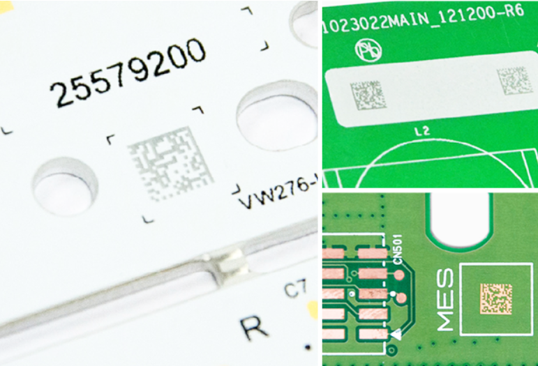
1. Suitable for marking traceability information such as barcode, QR code, and characters on the hard copper plate layer of PCBs in the fields of mobile phones, wearable devices, and automotive electronics.

2. Ultraviolet、Green、Infrared、CO2 laser is suitable.

3. Processing method could be single-faced marking, double-faced(built-in flap) marking, and double-faced(double laser heads) marking.

PCB Cutting

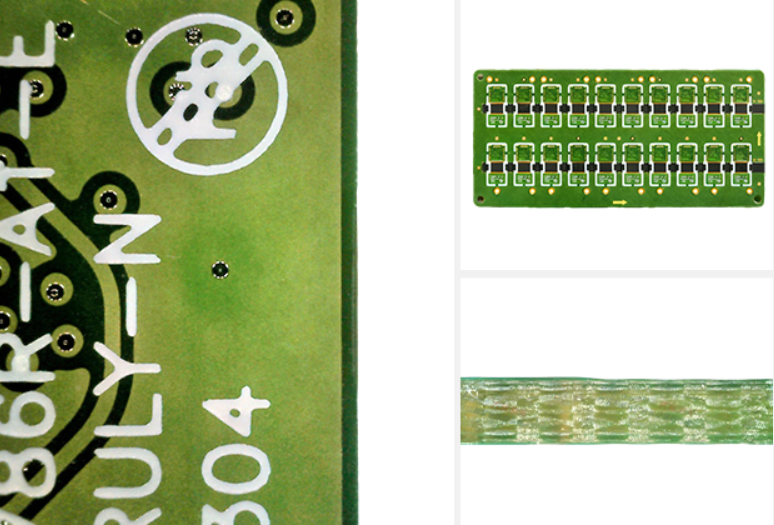
1. Non-contact process: Eliminates mechanical stress and deformation.

2. Ideal for any shape: Produces no dust, a narrow kerf, and a small heat-affected zone.

3. Full imported vision system: Ensures high precision for effectively processing high-density, high-integration PCBs.

FPCA Cutting

1. Non-contact process: Eliminates mechanical stress and deformation.

2. Ideal for any shape: Produces no dust, a narrow kerf, and a small heat-affected zone.

3. Full imported vision system: Ensures high precision for effectively processing high-density, high-integration PCBs.


Send us an Inquiry

.....Or contact us via Whstapp